


Brain Tumor Detection Using MRI Segmentation
Challenges
- Medical imaging plays a pivotal role in diagnosing and planning treatment for brain tumors, which affect millions globally. Accurate segmentation and classification of brain tumors from medical images are crucial to assist clinicians in understanding tumor characteristics.
- A client required an AI-powered solution to improve brain tumor diagnosis. The main challenge was the time-consuming and complex manual process of delineating tumor boundaries and classifying different tumor types. The objective is to explore 2D Image Segmentation using neural networks for brain tumor classification and segmentation.
Industry
Healthcare & Medical Imaging
Outcome
- The AI-powered brain tumor segmentation solution significantly improves diagnostic accuracy, reducing manual effort and analysis time.
- Clinicians benefit from enhanced workflow efficiency, faster tumor identification, and improved treatment planning.
Restaurant Analytics and Insights Dashboard
Challenges
- Obtain a comprehensive view of restaurant performance across multiple dimensions, including price segments, customer ratings, and operational timings.
- Identify key trends and insights such as popular dining times, top restaurant types, and highperforming chains and districts.
Industry
Restaurants (Cloud Kitchen)
Outcome
- Enhanced visibility into performance across various restaurant segments and geographic areas.
- Empowered decision-makers to fine-tune marketing strategies, operational hours, and menu offerings based on actionable insights.
Crafting Perfection with AI Resume Parser
Challenges
- Improve a candidate’s chances of landing an interview by optimizing their resume.
- Align resumes with job descriptions to meet ATS (Applicant Tracking System) requirements.
- Help job seekers highlight relevant skills and experiences based on employer expectations.
Industry
Human Resources & Recruitment, Career Development & Job Portals, Education & Professional Training
Outcome
- Higher job interview success rates through tailored resume optimization.
- Improved ATS compatibility, ensuring resumes pass automated screenings.
- Better candidate-employer alignment, reducing hiring mismatches.
Market Share and Sales Trends in the Total US Market
Challenges
- Understanding changes in market share and online sales penetration across various product categories.
- Identifying growth or decline trends among different manufacturers and sectors.
- Adapting business strategies in response to shifts in consumer purchasing behaviors.
Industry
Marketing/Sales
Outcome
- Detailed understanding of market share dynamics and online sales penetration.
- Identification of strong and weak performing categories and manufacturers.
- Enhanced strategic decision-making based on consumer trends and performance analysis.
Multi-script Text Detection From Sign Board Images
Challenges
- Multi-script text detection and recognition are crucial in computer vision and AI.
- Supports text translation systems or mobile-based OCR in multi-script environments.
- Accurate multi-script text detection from images is challenging and requires advanced techniques.
Industry
Smart Vision Systems, Multilingual AI Solutions, and Smart City Infrastructure
Outcome
- Model integration into a Web App enables defect and text detection.
- Efficient multilingual text detection from signboard images.
- Improved recognition accuracy for selected languages.
- Local language identification enhances understanding.
AI Powered Interview System
Challenges
- Reduced Hiring Time & Cost – Automates first-round interviews, eliminating human intervention and quickly filtering unsuitable candidates.
- Role-Specific Questioning – Generates customized questions based on the candidate’s role, ensuring relevant assessments.
- Fair & Unbiased Hiring – Eliminates human inconsistencies with standardized AI driven evaluation.
Industry
Recruitment, Human Resource & Talent acquisition
Outcome
- Faster & more efficient hiring with minimal recruiter involvement.
- More productive HR teams, as employees are not occupied with repetitive screenings.
- Improved Candidate Experience – Ensures a structured, engaging, and role-specific interview process.
- Fair, structured, and unbiased candidate evaluation.
Healthcare Financial Management System Enhancement
Challenges
- A healthcare provider faced challenges in efficiently tracking and managing financial operations and patient flow across various facilities
- The primary objectives were to improve the monitoring of collections and patient handling efficiency, enhance financial forecasting, and optimize resource allocation.
Industry
Outcome
- The solution involved developing a comprehensive dashboard to visualize key performance indicators across different metrics such as Collections per Hour, Patients per Hour, New and Existing Patients, and Monthly Financial Data. The dashboard allowed for comparisons across different years and doctors, facilitating a deeper understanding of trends and variances.
Transforming Spaces with Innovative Interior Design Visualization App
Challenges
- A client approached us with a common but significant challenge – the inability to visualize and conceptualize how different furniture styles would complement rooms and various spaces within the homes. Lacking inspiration, they found it challenging to make informed decisions about furniture selection and placement.
- They asked us to create an innovative AI-powered Interior Design app that seamlessly displays diverse styles and trends based on uploaded images of a given space. The app produces visually stunning output images featuring the selected furniture style, providing users with a rich preview of how their chosen design would come to life within the space.
Industry
Interior Design & Home Decor
Outcome
- Enhanced Customer Decision-Making – Realistic visualizations empower users to confidently choose furniture styles that fit their spaces.
- Increased Sales Conversion – Improved visualization leads to higher purchase intent, reducing hesitation in furniture buying.
- Reduced Product Returns – Accurate previews minimize mismatched expectations, lowering return rates and associated costs.
- Improved User Engagement – Interactive and immersive design exploration keeps users engaged longer, enhancing brand loyalty.
Container Defects Detection System for a Global Port Operator
Challenges
- Automate the inspection process for shipping container defects – Implement automated systems to streamline defect identification.
- Reduce the labor-intensive and time-consuming nature of manual container inspections – Cut down on hours spent by human inspectors and speed up throughput.
- Minimize human error in defect detection due to task complexity and repetition – Use consistent automated checks to lower missed or misclassified defects.
- Improve the accuracy of identifying various types of container defects – Leverage advanced detection algorithms to spot corrosion, dents, cracks, and seal failures precisely.
Industry
Logistics & Transportation.
Outcome
- The model integration combines the trained models to detect defects in the container.
- The system streamlines the container inspection process, reducing time and resource requirements.
- The solution eliminates the risk of missed defects that often occur during manual inspections.
- The system rapidly identifies defects as containers are processed, preventing defective containers from entering the supply chain.
Reshaping Yard Management Systems with Efficient Container Placement
Challenges
- With over 25,000 container locations, manually comparing and optimizing each one is impractical and time-consuming.
- The yard management system must account for diverse criteria, including size, occupancy, import/export type, temperature requirements, and staying durations, making the optimization process highly intricate.
- Efficiently assigning optimum positions to incoming containers in a vast yard poses a significant challenge.
- Containers with the same ID may have different staying durations in the yard, further complicating the optimization task.
Industry
Logistics & Supply Chain Management
Outcome
- Reduced Container Movement Time – Optimized container placement minimizes travel distance, leading to faster handling and reduced operational costs.
- Minimized Yard Congestion – Strategic placement reduces bottlenecks, improving overall yard flow and operational productivity.
- Reduced Manual Effort – Automation eliminates the need for manual container allocation, significantly reducing labor costs and human error.
AI-Driven Dynamic Pricing Optimization
Challenges
- Maximize revenue through optimized dynamic pricing strategies.
- Enable real-time price adjustments based on market demands.
- Improve pricing control through data analysis and machine learning techniques.
Industry
E-commerce & Retail
Outcome
- Optimized pricing strategies help maximize earnings by balancing demand and profitability.
- AI-driven demand predictions ensure competitive pricing, leading to more bookings.
- Automates price adjustments, reducing manual efforts in pricing management.
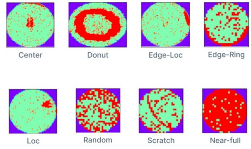
Machine Learning-Based Solution to Detect Defects In Semiconductor Manufacturing Process
Challenges
- To automate the visual inspection process of wafer surfaces in semiconductor manufacturing.
- To address the increasing complexity and density of semiconductor components.
- To improve accuracy and efficiency in defect detection and identification.
Industry
Semiconductor Industry
Outcome
- The machine learning-based solution for wafer defect detection and categorization improves the quality of the final product by identifying and addressing defects that might otherwise go unnoticed, leading to reduced product returns.
- The system reduces production costs by streamlining the inspection process and minimizing the need for manual labor.
Abstract-based Sentiment Analysis System for the Hospitality Industry
Challenges
- Service Improvement – Identify areas of concern and enhance service quality based on feedback.
- Customer Insights – Extract key sentiments from reviews to understand guest experiences and preferences.
Industry
Hospitality and Tourism
Outcome
- Early Detection of Emerging Trends – Identifies shifts in customer sentiment over time, allowing businesses to adapt to changing preferences and market demands before competitors.
- Crisis Management & Reputation Control – Detects sudden spikes in negative sentiment, enabling businesses to address issues before they escalate into full-blown PR crises.
AI Meeting Summary Tool for Organizational Excellence
Challenges
- Improve meeting efficiency by eliminating the need for manual note-taking.
- Ensure seamless knowledge sharing and alignment across teams.
- Reduce information loss and miscommunication in fast-paced work environments.
Industry
Information Technology & Software Development
Outcome
- Increased productivity by reducing time spent on manual note-taking and follow-ups.
- Ensure seamless knowledge sharing and alignment across teams.
- Enhance decision-making by providing well-structured meeting insights.
Text-to-Image Generation for Fashion Ideas
Challenges
- Automate the initial design visualization process.
- Reduce time-to-market for new fashion concepts.
- Enable rapid prototyping of fashion designs.
Industry
Fashion Technology, E-Commerce, Retail
Outcome
- Time Efficiency – Reduced design visualization time from days to minutes, decreased iteration cycles from hours to minutes, and accelerated stakeholder feedback.
- Cost Reduction – Eliminated the need for initial physical prototypes and reduced designer hours for concept visualization by minimizing revision cycles.
- Productivity Improvements – Multiple design variations can be generated simultaneously, reducing time-to-market for new designs.
- Design Process Enhancement – Improved creative exploration capabilities by providing freedom for more experimental design.
Automated Housekeeping Auditing Of Properties In Hospitality
Challenges
- Automate Housekeeping Audits Using AI
- Reduce Operational Costs and Increase Efficiency
- Optimize Housekeeping Resource Allocation
Industry
Hospitality & Facility Management
Outcome
- Increased Operational Efficiency – Faster room turnover and optimized staff utilization.
- Cost Reduction – Lower labor costs by minimizing manual inspections.
- Improved Guest Satisfaction – Higher cleanliness standards leading to better reviews.
- Standardized Quality Control – Consistent housekeeping performance across multiple locations.